Effective mass concept
The effective mass concept addressed here descends from the similarity with the acceleration of a body with mass m* and
the acceleration experienced by a free electron (or hole) due to an external force. In general, the thereby obtained
effective mass is a tensor and depends on the inverse curvature of the electron energetic states versus electron momentum
dispersion (m*)ij ~ (1/d2E/dkidkj). The free-carrier optical response of n- or p-type
zincblende III-V materials, for instance, originates from the zincblende Ga-point
conduction-band (single-valley, single-band) Bloch electrons, or valence-band holes (single-valley, multiple-band) near
the respective Fermi-level location. In particular, m* provides the electron(hole)-momentum-dependent curvature of the
conduction(valence) band(s), which are important physical material parameters, to which results from calculation schemes
such as kp-methods have to be compared.
AlGaInP
AlGaInP is of highest current technological importance for high-power, high-luminescent solid state light emitters.
The physical properties such as the effective mass parameters, phonon modes, and electrical transport properties are
influenced by alloying, lattice-mismatch-induced strain and atomic ordering. AlGaInP can be grown lattice matched to
GaAs using metal organic vapor phase deposition, and under certain growth conditions spontaneous long range ordering
can be avoided. The Ga-point hole and electron effective mass parameters have
not yet been determined experimentally for unstrained, disordered AlGaInP, and we have embarked to study these parameters
by use of far-infrared magneto-optic ellipsometry. Mueller matrix spectra of a n-GaAs/n-AlGaInP/i-GaAs layer structure
are shown in Fig. 2.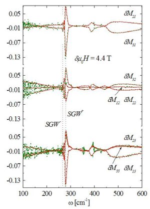
Fig. 2.
The spectra are differences between those taken at B = -3T and B = +3T,
and reflect the MO-induced birefringence within the differently conductive Te-doped n-GaAs cap layer (approximately 50nm thick)
and the n-AlGaInP layer (~1900nm). Modelling of the ellipsometric parameters provides N, m*, and m
for both layers independently (T. Hofmann, M. Schubert, C. M. Herzinger, I. Pietzonka, Appl. Phys. Lett. 82, 3463 - 3465
(2003))
< previous
|
|
InGaNAs and BGaInAs
The nitrogen and boron diluted InGaAs compounds are promising candidates for NIR absorber materials in multijunction-solar-cell
or detector structures, and for active materials in NIR laser diodes. Due to the smaller covalent radii of nitrogen and
boron compared with the substituted element, the lattice-mismatch induced strain in InGaAs, when grown on GaAs, can be
partially or completely compensated allowing for growth of thick layers. Sufficient n- and p-type doping is a prerequisite
for successful fabrication of p-n-junctions. Considerable effort was spent in the last few years concerning growth and
optical properties of InGaNAs, less information on systematic doping studies are available, little is known about the
physical material properties of BInGaAs. In essence, incorporation of nitrogen in InGaAs causes a dramatic red-shift of
the band edge. This effect is explained by nitrogen-induced cluster states within the band gap and perturbed host states
within the Ga-point conduction band edge. The perturbed host states overtake
the band gap states upon increasing nitrogen concentration accompanied by drastic down shift of their energetic levels.
Associated with these amalgamated band gap states is a strong increase of the Ga-point
electron effective mass m*. In contrast, boron incorporation in InGaAs has only minor effects on the band edge.
A slight increase of the band-gap-energy of BGaAs with increasing boron incorporation was reported. For BGaAs a
relatively small and composition independent band gap bowing was predicted.
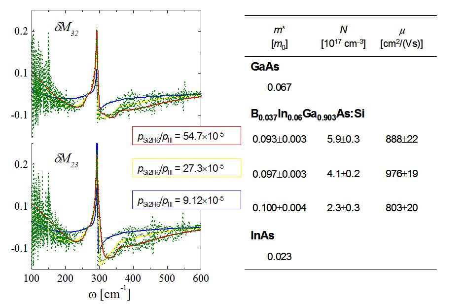
Fig. 3
depicts selected MO-mueller-matrix difference spectra for three different Si-doped n-type BInGaAs layers deposited by MOCVD
on undoped GaAs, for varying silane pressures. With increasing carrier concentration N, the effective mass reduces, and is much larger
than expected for unstrained InGaAs (T. Hofmann, G. Leibiger, N. Ashkenov, V. Gottschalch, M. Schubert, Strong increase of
the electron effective mass in GaAs incorporating boron and indium, submitted for publication in Phys. Rev.).
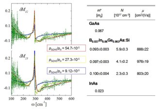 Fig. 3.
Collaborators: Osram Opto Semiconductors GmbH Regensburg (Dr. Ines Pietzonka, Dr. Klaus Streubel), Faculty of Chemistry
and Mineralogy, University Leipzig (Dr. Volker Gottschalch, Dr. Gunnar Leibiger), University of Nebraska-Lincoln, U.S.A. ( Prof. Dr. J.A. Woollam)
Funding: Deutsche Forschungsgemeinschaft (SCHUH 1338/3-1)
|