Magneto-optic Hall effect |
The free-carrier-properties effective mass m*, mobility m, and carrier concentration N are of fundamental importance for understanding basic material properties of semiconductors. N, m*, and m intriguingly combine concepts of classical (such as the effective "inertial" carrier mass) and quantum physics (e.g., the energy-momentum-dispersion and band occupation). A long term goal has been the accurate and simultaneous measurement of N, m, and m* by non-contact optical means in materials which are part of complex layered systems, such as semiconductor heterostructures.
Commonly, the electrical Hall-effect is measured to access N and m, which requires ohmic contacts. Such measurements are difficult if the material of interest is part of a complex layer structure, eventually buried by other highly-resistive or differently-conductive layers. The correct interpretation of the electrical measurement requires furthermore exact knowledge of the contact geometry, because Schottky barrier formation or space charge accumulation potentially affect the results.
According to the Drude model, the dielectric function e provides access to the square of the free-carrier (unscreened) plasma frequency wp and plasma resonance broadening gp. Under simplified assumptions about the free-carrier momentum distribution function - a single-species-carrier-plasma taken as example - wp and gp translate into the coupled quantities N/m* and m*m. No distinction can be made between N, m*, and m from measurement of e alone, nor can the sign of q be determined because wp is proportional to |q|. However, when brought into a magnetic field, the Lorentz force renders e a complex tensor, and provides the additional information required to obtain m* and sign(q). For semiconductor materials, this can be done by measurement of the magnetic-field-induced free-carrier birefringence. This approach is also applicable to organic conducting materials.
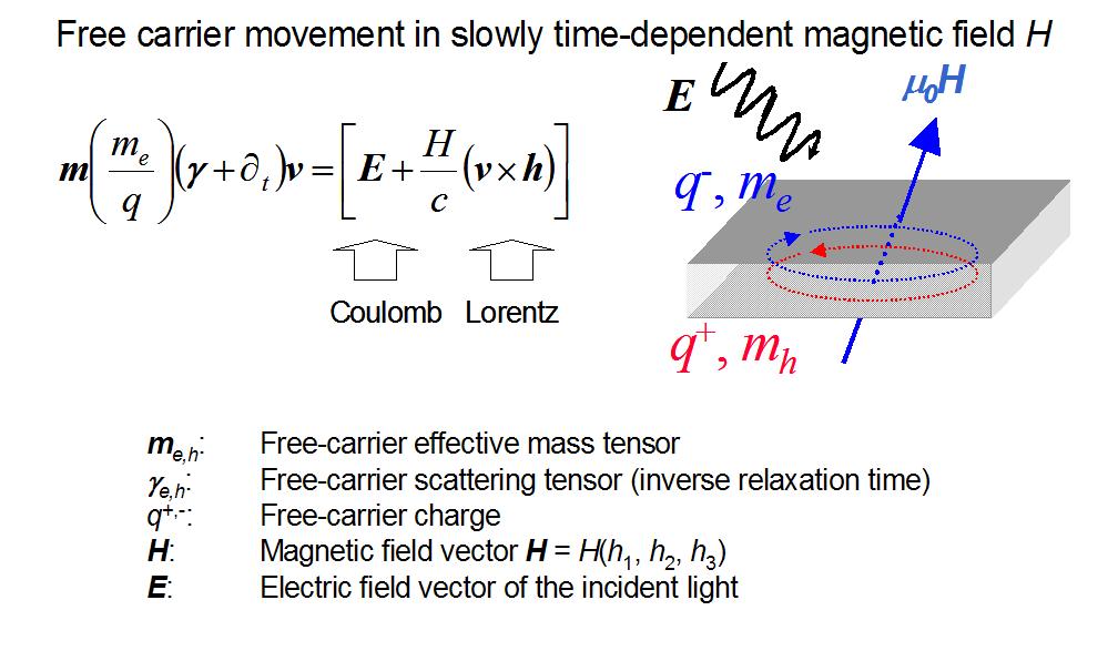 Fig. 0.
Generalized Ellipsometry
Standard (isotropic) ellipsometry determines two independent parameters, which provide the dielectric function e avoiding the Kramers-Kronig extension of pure intensity spectra in order to access both real and imaginary parts of e . Generalized ellipsometry extends to arbitrarily anisotropic materials, and allows for determination of the complete e tensor. Six parameters, which consist of the elements of the Jones reflection matrix, can be measured. The Jones matrix depends on the sample structure, each sample constituent's e, the ambient index of refraction, and the angle of incidence Fa. Treatment of anisotropic media is alternatively done within the Mueller-matrix- and Stokes-vector-approach. The elements of e follow by comparing calculated data to measured data upon standard least-square fit procedures. In addition to the ellipsometric parameters their standard deviations are determined, and propagated into the uncertainties (standard error) of the resulting fit parameters.
Far-infrared magneto-optic (MO) ellipsometer
Our setup uses a superconducting magnetocryostat (Oxford) with optical access ports and temperature-controlled (4K - RT) sample holder (Fig. 1. The magnetocryostat is kindly provided by Professor Dr. Pablo Esquinazi.) The magnetic field is parallel to the incident beam direction, and the angle of incidence is 45°. The strength of the field can be varied between B = -6T ... 6T. The beam is guided through exterior and interior windows, made from diamond and polyethylene. A third set of windows allows for transmission-type measurements. Details of a previous setup are given in M. Schubert, T. Hofmann, C. M. Herzinger, J. Opt. Soc. Am. A 20, 347 - 356 (2003).
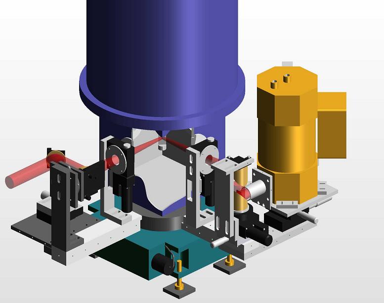 Fig. 1.
Effective mass concept
The effective mass concept addressed here descends from the similarity with the acceleration of a body with mass m* and the acceleration experienced by a free electron (or hole) due to an external force. In general, the thereby obtained effective mass is a tensor and depends on the inverse curvature of the electron energetic states versus electron momentum dispersion (m*)ij ~ (1/d2E/dkidkj). The free-carrier optical response of n- or p-type zincblende III-V materials, for instance, originates from the zincblende Ga-point conduction-band (single-valley, single-band) Bloch electrons, or valence-band holes (single-valley, multiple-band) near the respective Fermi-level location. In particular, m* provides the electron(hole)-momentum-dependent curvature of the conduction(valence) band(s), which are important physical material parameters, to which results from calculation schemes such as kp-methods have to be compared.
AlGaInP
AlGaInP is of highest current technological importance for high-power, high-luminescent solid state light emitters. The physical properties such as the effective mass parameters, phonon modes, and electrical transport properties are influenced by alloying, lattice-mismatch-induced strain and atomic ordering. AlGaInP can be grown lattice matched to GaAs using metal organic vapor phase deposition, and under certain growth conditions spontaneous long range ordering can be avoided. The Ga-point hole and electron effective mass parameters have not yet been determined experimentally for unstrained, disordered AlGaInP, and we have embarked to study these parameters by use of far-infrared magneto-optic ellipsometry. Mueller matrix spectra of a n-GaAs/n-AlGaInP/i-GaAs layer structure are shown in Fig. 2. The spectra are differences between those taken at B = -3T and B = +3T, and reflect the MO-induced birefringence within the differently conductive Te-doped n-GaAs cap layer (approximately 50nm thick) and the n-AlGaInP layer (~1900nm). Modelling of the ellipsometric parameters provides N, m*, and m for both layers independently (T. Hofmann, M. Schubert, C. M. Herzinger, I. Pietzonka, Appl. Phys. Lett. 82, 3463 - 3465 (2003))
 Fig. 2.
InGaNAs and BGaInAs
The nitrogen and boron diluted InGaAs compounds are promising candidates for NIR absorber materials in multijunction-solar-cell or detector structures, and for active materials in NIR laser diodes. Due to the smaller covalent radii of nitrogen and boron compared with the substituted element, the lattice-mismatch induced strain in InGaAs, when grown on GaAs, can be partially or completely compensated allowing for growth of thick layers. Sufficient n- and p-type doping is a prerequisite for successful fabrication of p-n-junctions. Considerable effort was spent in the last few years concerning growth and optical properties of InGaNAs, less information on systematic doping studies are available, little is known about the physical material properties of BInGaAs. In essence, incorporation of nitrogen in InGaAs causes a dramatic red-shift of the band edge. This effect is explained by nitrogen-induced cluster states within the band gap and perturbed host states within the Ga-point conduction band edge. The perturbed host states overtake the band gap states upon increasing nitrogen concentration accompanied by drastic down shift of their energetic levels. Associated with these amalgamated band gap states is a strong increase of the Ga-point electron effective mass m*. In contrast, boron incorporation in InGaAs has only minor effects on the band edge. A slight increase of the band-gap-energy of BGaAs with increasing boron incorporation was reported. For BGaAs a relatively small and composition independent band gap bowing was predicted.
Fig. 3 depicts selected MO-mueller-matrix difference spectra for three different Si-doped n-type BInGaAs layers deposited by MOCVD on undoped GaAs, for varying silane pressures. With increasing carrier concentration N, the effective mass reduces, and is much larger than expected for unstrained InGaAs (T. Hofmann, G. Leibiger, N. Ashkenov, V. Gottschalch, M. Schubert, Strong increase of the electron effective mass in GaAs incorporating boron and indium, submitted for publication in Phys. Rev.).
 Fig. 3.
Collaborators: Osram Opto Semiconductors GmbH Regensburg (Dr. Ines Pietzonka, Dr. Klaus Streubel), Faculty of Chemistry and Mineralogy, University Leipzig (Dr. Volker Gottschalch, Dr. Gunnar Leibiger), University of Nebraska-Lincoln, U.S.A. ( Prof. Dr. J.A. Woollam)
Funding: Deutsche Forschungsgemeinschaft (SCHUH 1338/3-1)
| back to Research |